Malaysia’s Front-End GaN Semiconductor Technology Partner

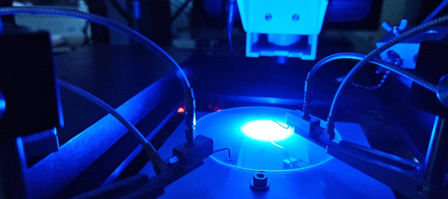
GaN-based semiconductor offers superior performance for optoelectronics, high-power and RF applications but it is difficult to manufacture because it is grown on mismatched substrates leading to strain, crystal defects, and wafer bow, especially at above 6-inch wafer scale. We, Kirana Semikonduktor succeeds because it is led by deep GaN epitaxy experts who developed GaN from first principles, identifying critical strain-controlling layers and interfaces, enabling uniform, low-defect, cost-effective, and scalable industrial-grade GaN manufacturing.
Our recipe is proven faster and more efficient compare to other competitors. The advantage is not the machines, but our deep know-how in controlling the process which is the RECIPES. This allows us to make high-quality GaN wafers at lower cost. Right now, we produce small wafers (2-inch and 4-inch) in the lab. The next important step is to scale up to 6-inch wafers so they can be used by industry. Our understanding of material stress, defects, and layer interfaces helps create GaN devices that perform better, can be produced at larger scale, and cost less than those from major global manufacturer
KIRANA GaN TEMPLATE


Over 20 years of experience in Nitride-based research
100+ publications in hi-index journals
Hold more than 5 IPs in semiconductor technology
Supervised more than 10 postgraduates students
10+ years of experience in Nitride-based semiconductor technologies in both academic and industry
3 years in LEDs industries as Staff Epitaxial GaN Process Engineer
30 publications in h-index journals
Hold 1 IP in semiconductor technology
Supervised more than 5 postgraduates
Assoc. Prof. Dr. Norzaini Zainal
Ts. Dr. Mohd Nazri Abd Rahman
MEET THE GaN EXPERTS

Mohd Anas Ahmad
15+ years of experience in optimizing and maintaining semiconductor processes
200+ publications in h-index journals
Hold more than 5 IPs in semiconductor technology

Contact Us
Kirana Semikonduktor Sdn. Bhd.
CR5, Block A, sains@usm Bukit Jambul,
11900 Bayan Lepas, Penang, MY
kiranasemikonduktor@gmail.com
+604-6535637
© 2025. All rights reserved.